Product Summary
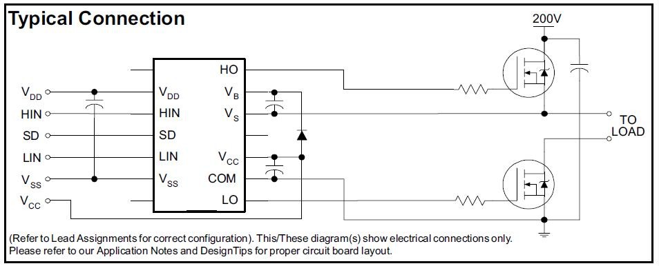
The IR2010 is a high power, high voltage, high speed power MOSFET and IGBT driver with independent high and low side referenced output channels, ideal for Audio Class D and DC-DC converter applications. Logic inputs of IR2010 are compatible with standard CMOS or LSTTL output, down to 3.0V logic. The output drivers feature a high pulse current buffer stage designed for minimum driver cross-conduction. Propagation delays are matched to simplify use in high frequency applications. The floating channel can be used to drive an N-channel power MOSFET or IGBT in the high side configuration which operates up to 200 volts. Proprietary HVIC and latch immune CMOS technologies enable ruggedized monolithic construction. The applications of the IR2010 include Audio Class D amplifiers, High power DC-DC SMPS converters, Other high frequency applications.
Parametrics
IR2010 absolute maximum ratings: (1)High side floating supply voltage: -0.3 to 225 V; (2)High side floating supply offset voltage: VB - 25 to VB + 0.3; (3)High side floating output voltage: VS - 0.3 to VB + 0.3; (4)Low side fixed supply voltage: -0.3 to 25 V; (5)Low side output voltage: -0.3 to VCC + 0.3 V; (6)Logic supply voltage: -0.3 to VSS + 25 V; (7)Logic supply offset voltage: VCC - 25 to VCC + 0.3 V; (8)Logic input voltage (HIN, LIN & SD): VSS - 0.3 to VDD + 0.3 V; (9)Allowable offset supply voltage transient: 50 V/ns; (10)Package power dissipation @ TA ≤ +25℃: (14 lead DIP): 1.6 W, (16 lead SOIC): 1.25 W; (11)Thermal resistance, junction to ambient (14 lead DIP): 75 ℃/W, (16 lead SOIC): 100 ℃/W; (12)Junction temperature: 150 ℃; (13)Storage temperature: -55 to 150 ℃; (14)Lead temperature (soldering, 10 seconds): 300 ℃.
Features
IR2010 features: (1)Floating channel designed for bootstrap operation Fully operational to 200V; (2)Tolerant to negative transient voltage, dV/dt immune; (3)Gate drive supply range from 10 to 20V; (4)Undervoltage lockout for both channels; (5)3.3V logic compatible Separate logic supply range from 3.3V to 20V Logic and power ground ±5V offset; (6)CMOS Schmitt-triggered inputs with pull-down; (7)Shut down input turns off both channels; (8)Matched propagation delay for both channels; (9)Outputs in phase with inputs; (10)Also available LEAD-FREE.
Diagrams

| Image | Part No | Mfg | Description |  |
Pricing (USD) |
Quantity | ||||||||||||
|---|---|---|---|---|---|---|---|---|---|---|---|---|---|---|---|---|---|---|
 |
 IR2010 |
 Other |
 |
 Data Sheet |
 Negotiable |
|
||||||||||||
 |
 IR2010(S) |
 Other |
 |
 Data Sheet |
 Negotiable |
|
||||||||||||
 |
 IR2010PBF |
 International Rectifier |
 Power Driver ICs Hi&Lw Sd Drvr |
 Data Sheet |

|
|
||||||||||||
 |
 IR2010S |
 Other |
 |
 Data Sheet |
 Negotiable |
|
||||||||||||
 |
 IR2010SPBF |
 International Rectifier |
 Power Driver ICs |
 Data Sheet |

|
|
||||||||||||
 |
 IR2010STRPBF |
 International Rectifier |
 Power Driver ICs Hi&Lw Sd Drvr |
 Data Sheet |

|
|
||||||||||||
 (China (Mainland))


